← Build a Spider Robot with Arduino: A Fun and Educational DIY Project! Adeept hexapod spider robot kit for arduino with android app crawling OCL 150 Watt Modif: Transform Your Audio with Bass Mantap Techniques! modif power ocl 150 watt menjadi super ocl502 →
If you are searching about Can AI Truly Replace Human PCB Designers? you've came to the right web. We have 25 Images about Can AI Truly Replace Human PCB Designers? like An Ultimate Guide To Pcb Wiring And Layout - vrogue.co, PCB Trace Basics For PCB Designers | Reversepcb and also PCB designers share their experience in PCB design with BGA devices. Here you go:
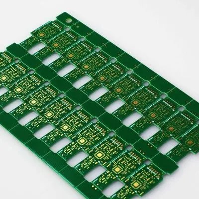
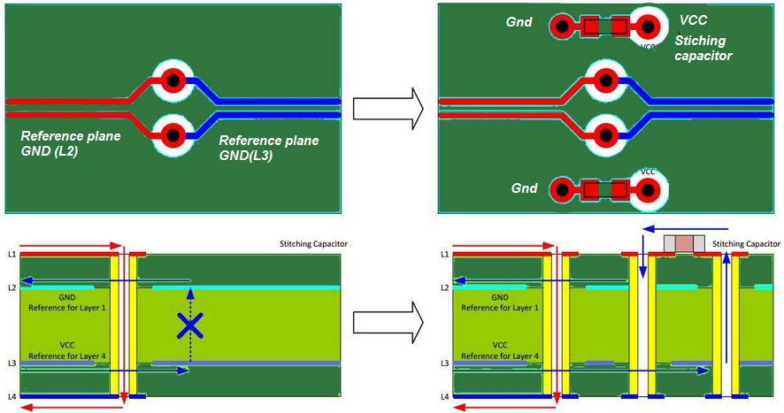
Can AI Truly Replace Human PCB Designers?
 southelectronicpcb.com
Can AI Truly Replace Human PCB Designers?
Guide To PCB Trace Length Matching In High Speed Design | NWES Blog
 www.nwengineeringllc.com
Guide to PCB Trace Length Matching in High Speed Design | NWES Blog
Main Design Guidelines & Layout Rules On High Speed PCB
 www.integrasources.com
Main Design Guidelines & Layout Rules on High Speed PCB
Podcast: PCB 3.0: SI/PI For PCB Designers - System, PCB, & Package
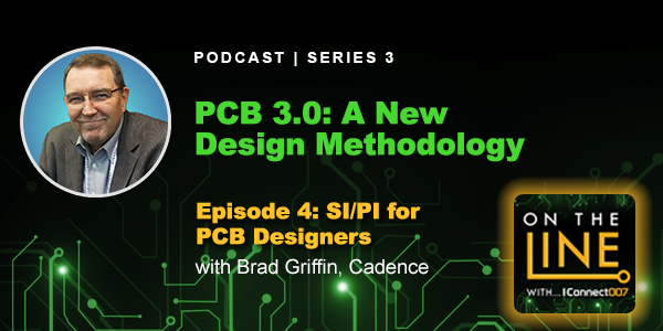 community.cadence.com
Podcast: PCB 3.0: SI/PI for PCB Designers - System, PCB, & Package ...
Pros And Cons Of Advanced Electronic Packaging For PCB Designers
Pros and Cons of Advanced Electronic Packaging for PCB Designers ...
Can AI Truly Replace Human PCB Designers?
 southelectronicpcb.com
Can AI Truly Replace Human PCB Designers?
Qualcomm Snapdragon APQ8016 Fanout
 fedevel.com
Qualcomm Snapdragon APQ8016 fanout
Focus On Embedded Development For PCB Designers | Altium
 resources.altium.com
Focus on Embedded Development for PCB Designers | Altium
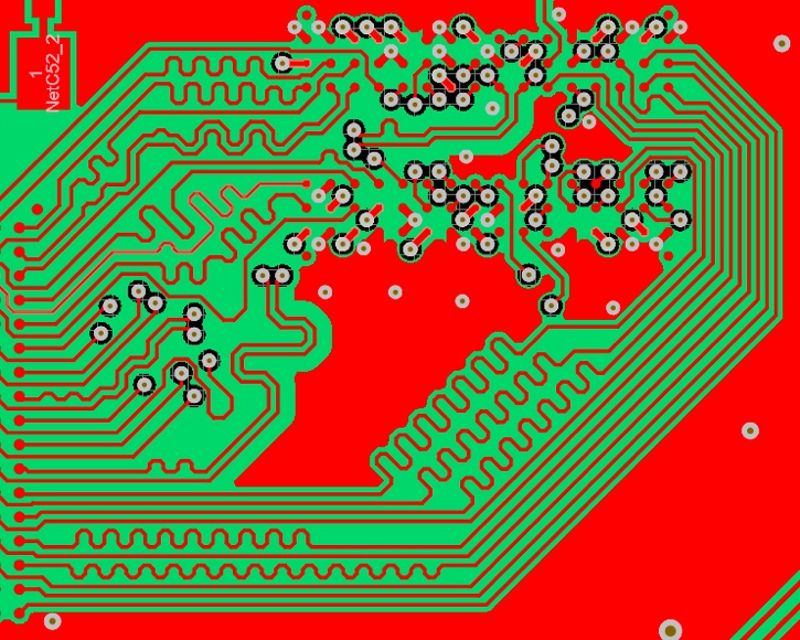
PCB Trace Basics For PCB Designers | Reversepcb
 reversepcb.com
PCB Trace Basics For PCB Designers | Reversepcb
Demystifying Standard FR4 Thickness: A Comprehensive Guide For PCB
 ksnpcb.com
Demystifying Standard FR4 Thickness: A Comprehensive Guide for PCB ...
Pcb Board Design Guide At Santiago Vanmatre Blog
 storage.googleapis.com
Pcb Board Design Guide at Santiago Vanmatre blog
Antenna Design Principles For PCB Designers
 www.linkedin.com
Antenna Design Principles for PCB Designers
PCB Designers PCB Circuit Board Assembly Wireless Charger PCBA - China
 newchip.en.made-in-china.com
PCB Designers PCB Circuit Board Assembly Wireless Charger PCBA - China ...
PCB Designers Share Their Experience In PCB Design With BGA Devices
 www.kingfordpcb.com
PCB designers share their experience in PCB design with BGA devices ...
Collaboration For Mechanical & PCB Designers | Guides | Altium 365
 resources.altium365.com
Collaboration for Mechanical & PCB Designers | Guides | Altium 365
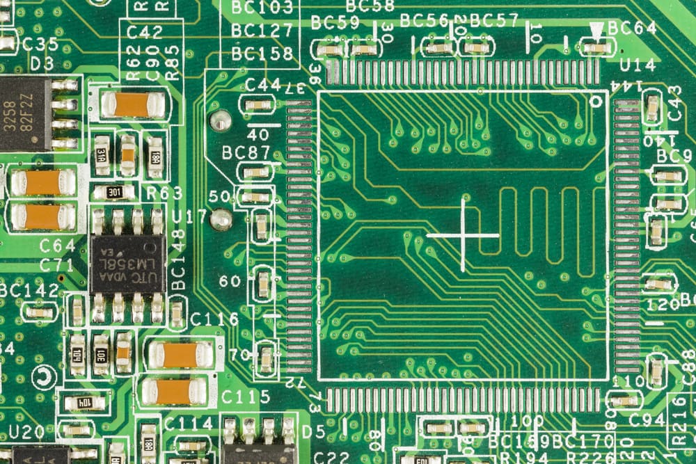
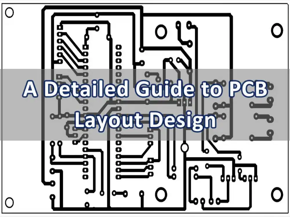
Complete Guide To PCB Layout Design Steps And Rules Circuit Diagram
 declanstarling.pages.dev
Complete Guide To PCB Layout Design Steps And Rules Circuit Diagram ...
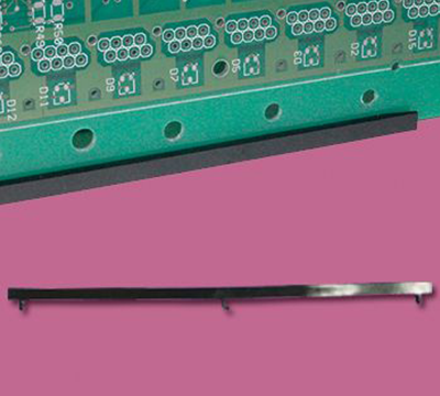
PCB GUIDE RAIL CG-21C
 www.plastlist.com
PCB GUIDE RAIL CG-21C
Why 98% Of Successful Pcb Designers Prioritize Effective Pcb Layout
 gighz.net
Why 98% of successful pcb designers prioritize effective pcb layout ...
Spanish PCB Design Landscape: University Origins & Regional Demand Trends
 www.linkedin.com
Spanish PCB Design Landscape: University Origins & Regional Demand Trends
PCB Designers To Contest For Design Champion Title At IPC APEX EXPO 2024
 www.pcbdirectory.com
PCB Designers to Contest for Design Champion Title at IPC APEX EXPO 2024
Advanced Pcb Layout Includes High Speed Layout - Andwin Circuits
 www.andwinpcb.com
Advanced pcb layout includes high speed layout - Andwin Circuits
An Ultimate Guide To Pcb Wiring And Layout - Vrogue.co
 www.vrogue.co
An Ultimate Guide To Pcb Wiring And Layout - vrogue.co
A Guide To PCB Card Guides, Ejectors And Pullers | Essentra Components UK
A guide to PCB card guides, ejectors and pullers | Essentra Components UK
11 Best High-Speed PCB Routing Practices – PCB HERO
 www.pcb-hero.com
11 Best High-Speed PCB Routing Practices – PCB HERO
Qualcomm Snapdragon APQ8016 Fanout
 fedevel.com
Qualcomm Snapdragon APQ8016 fanout
pcb trace basics for pcb designers. Demystifying standard fr4 thickness: a comprehensive guide for pcb. Main design guidelines & layout rules on high speed pcb